
A Comprehensive Guide to PCB Fabrication: Everything You Need to Know
- Gulshan Sharma
- Jan 21
- 4 min read

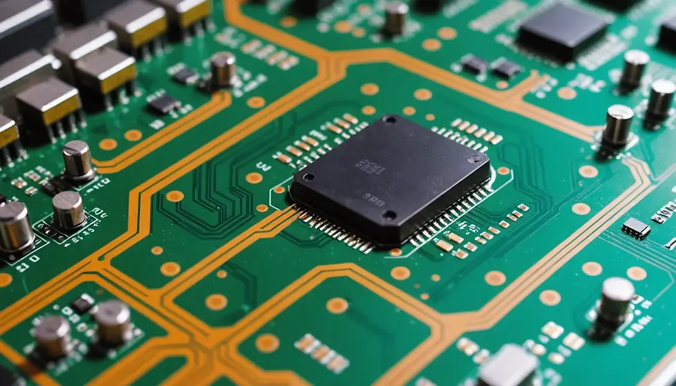
Printed Circuit Boards (PCBs) are the foundation of modern electronics, providing a structured platform for mounting and connecting electronic components. Whether it's a simple consumer device or a complex industrial system, PCBs are essential for electronic functionality. Understanding the PCB fabrication process, the necessary design files, and the different types and complexities of PCBs is crucial for ensuring optimal performance and manufacturability.

What is PCB Fabrication?
PCB fabrication refers to the manufacturing process that converts a conceptual electronic design into a physical board. This process involves multiple steps, from preparing design files to assembling and testing the final board. Successful PCB fabrication requires a precise understanding of materials, layers, and manufacturing techniques to produce boards that meet industry standards and performance expectations.
Essential Files for PCB Fabrication
To manufacture a PCB, a set of essential design files must be provided to the fabricator. These files are usually generated by PCB design software such as Altium Designer, Eagle, or KiCad. The key files required for PCB fabrication include:
Gerber Files: These industry-standard files contain information about copper layers, solder mask, silkscreen, and other board features.
Drill Files (Excellon Files): Specify the location and size of holes to be drilled on the PCB.
Bill of Materials (BOM): Lists all the electronic components required for assembly, including part numbers and quantities.
Pick-and-Place File: Provides information about the exact placement of components on the board for automated assembly.
Netlist: Describes the electrical connections between components to ensure proper functionality.
Fabrication Drawings: Provide mechanical and dimensional details for production.
Assembly Drawings: Guide the assembly process with component placement and orientation details.
Providing accurate and complete files ensures that the PCB is fabricated without errors and meets the intended design specifications.
Types of PCBs
PCBs come in various types based on the application, material, and structure. Choosing the right type of PCB is crucial for achieving optimal performance and reliability.
Single-Layer PCB:
Contains a single layer of conductive material.
Cost-effective and easy to manufacture.
Suitable for simple electronic devices such as calculators and LED circuits.
Double-Layer PCB:
Features conductive layers on both sides.
Provides more routing flexibility compared to single-layer boards.
Used in applications like automotive electronics and industrial controls.
Multilayer PCB:
Consists of three or more layers of conductive material.
Enables complex circuit designs with high functionality.
Common in aerospace, medical devices, and telecommunications.
Rigid PCB:
Made from solid, inflexible substrate materials like FR4.
Offers durability and mechanical stability.
Used in consumer electronics and industrial applications.
Flexible PCB:
Constructed from flexible materials such as polyimide.
Allows bending and folding for compact designs.
Ideal for wearable technology and medical devices.
Rigid-Flex PCB:
Combines rigid and flexible sections.
Reduces space and weight in advanced designs.
Found in military and aerospace applications.
High-Frequency PCB:
Designed for high-speed signal transmission.
Utilizes specialized materials like PTFE to reduce signal loss.
Common in RF and microwave applications.
Metal-Core PCB:
Contains a metal core (usually aluminum) for improved heat dissipation.
Used in LED lighting and power electronics.
PCB Layers and Their Importance
PCBs are classified based on the number of layers they contain. The complexity of the board depends on the number of layers and the design requirements.
1-2 Layers: Simple designs for basic applications.
4-8 Layers: Intermediate complexity, often used in embedded systems.
10+ Layers: High-density, multi-functional PCBs for critical applications like data centers and telecommunications.
Additional layers can improve signal integrity, allow for complex routing, and enhance performance in high-speed circuits.
Complexities in PCB Fabrication
PCB fabrication can become highly complex due to various factors, including:
Component Density: High-density designs require precise placement of components within limited board space.
Trace Width and Spacing: Fine-pitch traces demand advanced manufacturing capabilities.
Via Types: Use of through-hole, blind, buried, or microvias adds complexity.
Signal Integrity: High-speed designs must minimize noise and interference.
Thermal Management: Efficient heat dissipation is crucial for power-intensive applications.
Impedance Control: Maintaining impedance within tolerances is essential for high-frequency circuits.
Managing these complexities requires collaboration with experienced PCB fabricators to ensure design manufacturability and performance.
The PCB Fabrication Process
The PCB fabrication process involves several crucial steps:
Design Preparation: Reviewing design files for errors and manufacturability.
Material Selection: Choosing the appropriate substrate material.
Printing and Etching: Transferring the circuit design onto the substrate.
Drilling: Creating holes for mounting components and interlayer connections.
Plating: Adding conductive layers to drilled holes.
Lamination: Bonding multiple layers together.
Solder Mask Application: Protecting the board surface and defining solderable areas.
Silkscreen Printing: Adding component labels and identifiers.
Testing: Conducting electrical and mechanical tests for quality assurance.
Why Choose Professional PCB Fabrication Services?
Partnering with an experienced PCB fabrication service provider offers numerous benefits:
Precision and Consistency: Ensures accurate translation of design files into physical boards.
High-Quality Materials: Access to industry-standard materials.
Advanced Capabilities: Support for multilayer, high-density, and high-speed designs.
Quality Assurance: Comprehensive testing and validation to ensure reliability.
Conclusion
PCB fabrication is a crucial step in electronic product development that requires attention to detail and collaboration with reliable manufacturers. Understanding the types of PCBs, required design files, and fabrication processes can help streamline production and achieve high-quality results.
Ready to Get Started with PCB Fabrication?
Contact sales@xelec.in/ gulshan@xelec.in today to discuss your PCB fabrication needs and get a customized quote tailored to your project requirements.


Comments